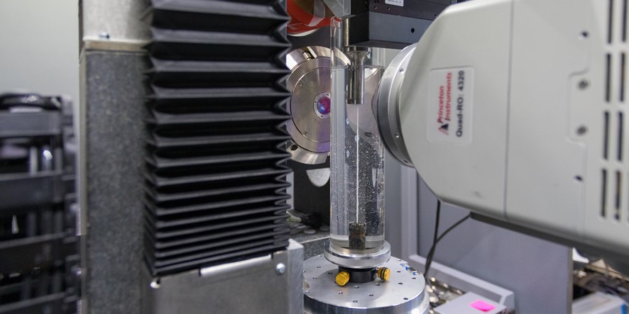
The transmission electron microscope is one of the leading research tool for the SIMAP lab. In 2013, a new FEG-TEM has been acquired with the help of the Labex CEMAM. This investment is strongly related to the development of the ACOM-TEM characterisation tool. Numerous projects are using this advanced facility.
Objectives
Development and validation of new TEM structural characterisation facilities. To provide structural information to analyse the physical processes related to the plastic deformation of metals and alloys, the precipitation mechanisms and/or the phase transformations.
The Automated Crystal Orientation Mapping (ACOM) tool
The spatial resolution is related to the detection limit of the boundaries between crystals. (JEOL 2100F)
The ACOM-TEM tool developed by E. Rauch (GPM2) and M. Véron (PM) and commercialized since 2009 by NanoMEGAS SPRL as ASTAR, provides phase and orientation maps at nanoscale, enables the identification of precipitates and distinguishes crystallized and amorphous components. It is based on the so-called template matching strategy that consists in comparing sets of pre-calculated diffraction patterns to the experimental signal either acquired in-situ with a dedicated camera or derived from high resolution (HRTEM) images through a Fourier transform. Around 80 ASTAR units are installed worldwide and more than 200 published works involve its usage. The spatial resolution accessible with the new JEOL 2100 FEG is 1 nm. Consequently, this TEM attachment is regularly exploited in the lab for structural characterisation at nanoscale. Around ten PhD works performed at SIMAP includes ACOM-TEM maps. The tool is constantly upgraded with new facilities.
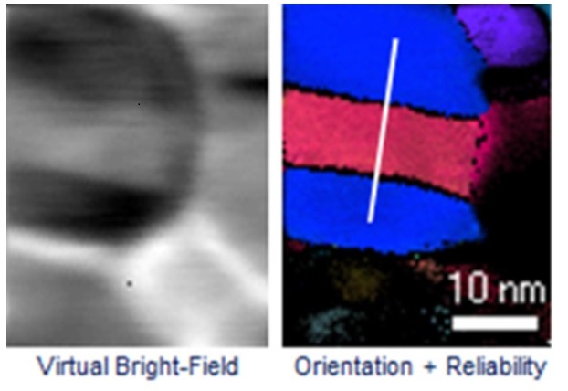
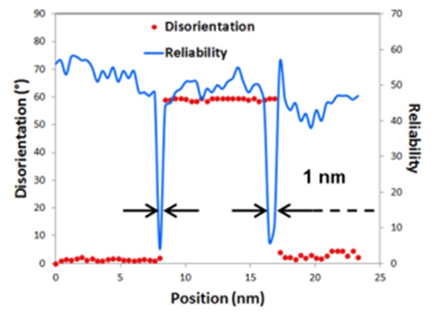
Amorphous phase detection
A nanoscale interconnect device. Two amorphous phases are recognized.
The template matching algorithm is efficient as long as a the material diffracting signature is known. In particular, the tool was adapted to amorphous phases. Indeed, the related diffraction patterns are composed of a main ring with a specific diameter that can be easily recognized. The figure below illustrates the capability of the tool to distinguish between crystallized and amorphous phases. This innovative technic is of particular interest for the microelectronics industry.
Virtual dark field images (VDF)
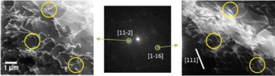
VDF images of deformed steel. Dislocations with the [111] Burgers vector (surrounded) are visible if g=[1?16] but not if g=[11?2] spot is selected to generate the image.
A huge amount of information may be retrieved off-line by taking advantage of the fact that all the diffraction patterns collected for a given ACOM-TEM scan are memorized. In particular virtual dark field images are reconstructed by extracting a freely selected fraction of the diffraction pattern. Such images are used to highlight structural features like dislocations.
Deconvolution of superimposed diffraction patterns
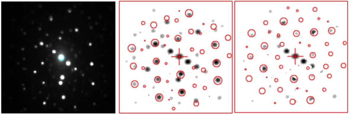
Successive template matching solutions with intermediate pattern subtraction. (Microscopy and Microanalysis (21/S3) 1243–1244)
For grain sizes lower than the thin foil thickness, the pattern is composed of superimposed reflection networks, each being related to a given grain crossed by the beam. To distinguish them, it has been proposed to subtract the spots related to first dominant crystal and to re-index the remaining pattern. The resulting algorithm is apply successively and was shown to be able to distinguish 3 to 5 grains in the sample thickness.
Selected Publications:
- M. Gemmi, M. G. I. La Placa, A. S. Galanis, E. F. Rauch and S. Nicolopoulos. ‘Fast electron diffraction tomography’ Appl. Cryst. (2015) 48, 718-727
- E.F. Rauch and M. Véron, “Virtual dark-field images reconstructed from electron diffraction patterns,” Eur. Phys. J. Appl. Phys., 66 10701 (2014).
- E. F. Rauch and M. Véron ‘Automated crystal orientation and phase mapping in TEM’ Materials Characterization 98 (2014) 1–9
- A. Valery, E. F. Rauch, A. Pofelski, L. Clément, F. Lorut ‘Dealing With Multiple Grains in TEM Lamellae Thickness for Microstructure Analysis Using Scanning Precession Electron Diffraction’ Microscopy and Microanalysis (21/S3) 1243 – 1244
- Moeck P, Rouvimov S, Rauch EF Véron M, Kirmse H., Häusler I., Neumann W. High spatial resolution semi-automatic crystallite orientation and phase mapping of nanocrystals in transmission electron microscopes, Crystal Research Tech. ,46/6, (2011) 589-606