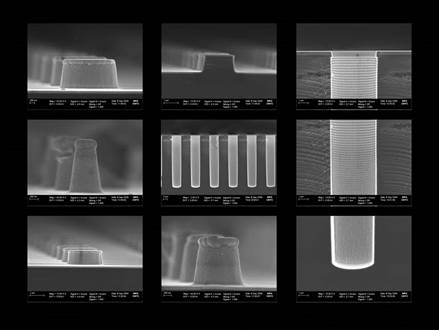
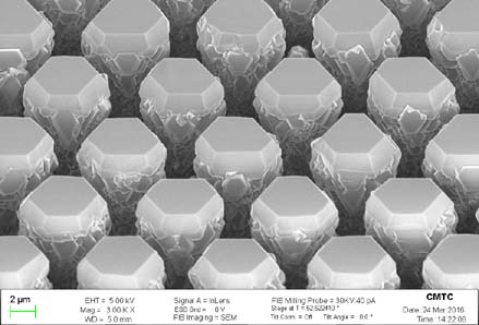
Various micrometric objects covered by the ALD technique (here TaN and Ta2O5)
4 inch silicon wafer covered with 80 nm of AlN (ALD technique)
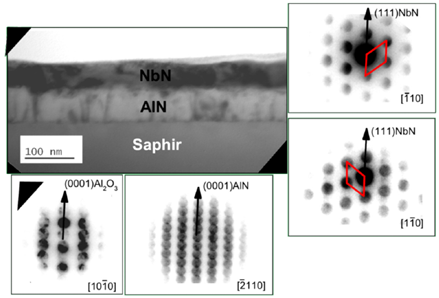
Multilayer of epitaxial nitrides and structure identification
Localised growth of epitaxial AlN on silicon pillars
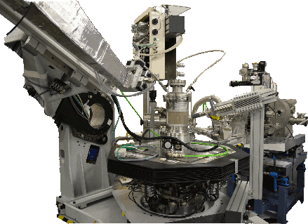
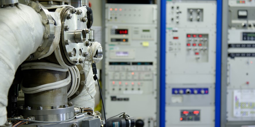
ALD/CVD reactor implemented on the diffractometer of the SIRIUS beamline at the French synchrotron SOLEIL (collaboration LMGP, SIMAP, SOLEIL, IM2NP, LMOPS)
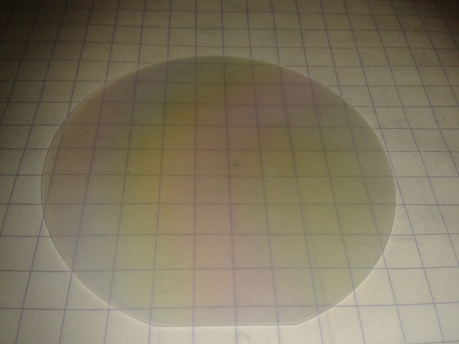
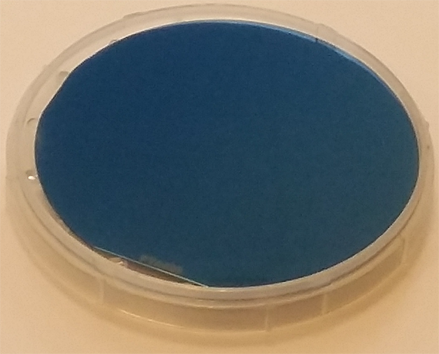
2 inch epitaxial AlN grown on sapphire by the Halide-CVD technique
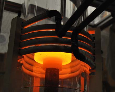
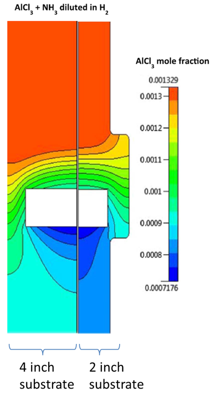
Halide CVD reactor at SIMAP
2 inch epitaxial NbN grown on sapphire by the Halide-CVD technique
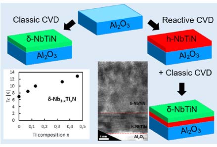
Superconducting properties of epitaxial NbTiN grown by Halide CVD
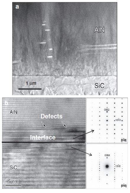
Atomic structure of the AlN/SiC interface