Research activities around additive manufacturing at SIMaP rely mainly on the Electron Beam Melting (EBM) technology. This technology enables to manufacture new designs and sophisticated geometries. This process is particularly suitable for the production of architectured materials such as lattice structures or metallic foams. A significant part of the activity is devoted to material development and especially to materials that show a poor weldability. Tailoring microstructures by playing with process parameters is the aim of undergoing research efforts.
Objectives
- Processing of complex architectured materials.
- Structural and mechanical characterization of the electron beam melted parts.
- Investigation of the effect of the process parameters on the microstructures and properties.
- Tailoring the microstructures by tuning process parameters and melting strategies.
- Specific optimizations for materials difficult to weld.
- Development of hybrid processes.
Architectured Ti-6Al-4V materials manufactured by EBM
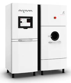
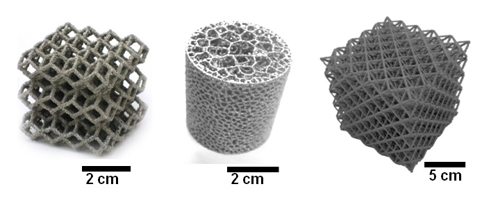
Left: EBM machine at SIMaP. Right: Examples of architectured Ti-6Al-4V materials produced by EBM
The biggest challenge of architectured materials was the processing route. With the recent development of additive manufacturing, it is now much easier to produce sophisticated geometries. SIMaP is now equipped with two EBM machines.
From the CAD file to the effective properties
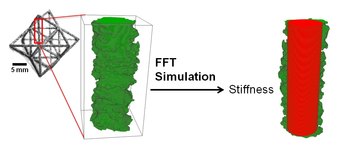
Illustration of the concept of mechanical efficiency. In red is highlighted the mechanical equivalent cylinder, i.e. a perfect cylinder having a stiffness equal to the as-built structure.
Lattice structures were produced by EBM and characterized structurally as well as mechanically. X-ray tomography was extensively used in order to characterize lattice structures in 3D. The discrepancies between the ideal properties (those of the CAD file) and the effective properties of the produced structure were investigated based on the concept of mechanical efficiency. This concept allows to discriminate the material that transmit loads with the one which doesn't.
surface defects and chemical etching
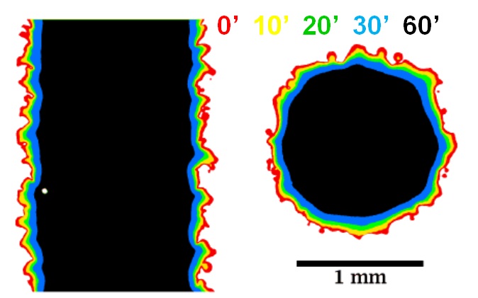
Effect of chemical etching on a single vertical strut as a function of the etching time.
Significant surface defects can be observed on as-built structures and are not considered as mechanically efficient. The effect of chemical etching on the surface defects was investigated. The chemical etching clearly improves the mechanical efficiency of the lattice structures. This is further illustrated in the above figure that shows the evolution of the strut morphology as a function of etching time. The surface profile after a 30 min etching time appears much smoother than the as-built profile.
Selected Publications:
- C. De Formanoir, M. Suard, R. Dendievel, G. Martin, S. Godet. Improving the mechanical efficiency of electron beam melted titaniul mattices structures by chemical etching. Additive Manufacturing, vol 11 (2016) 71-76
- G. Martin, D. Fabrègue, F. Mercier, J-A. Chafino-Aixa, R. Dendievel, J-J. Blandin. Coupling Electron Beam Melting and Spark Plasma Sintering: A new processing route for achieving architectured microstructures. Scripta Materialia vol 122 (2016)
- M. Suard, G. Martin, P. Lhuissier, R. Dendievel, F. Vignat, J-J. Blandin, F. Villeneuve. Mechanical equivalent diameter of single struts for the stiffness prediction of lattice structures produced by Electron Beam Melting. Additive Manufacturing, vol 8 (2015) 124-131
Chercheurs / Enseignants-chercheurs
PhD and post-docs
Edouard Chauvet,
Pierre-Thomas Doutre,
Antalia Ho-shui-lin,
Sébastien Pinson,
Guillaume Croset,
Hélène Gomez,
Akash Sonawane,
Alizée Thomas,
Alexis Burr
Emeric Plancher
Pierre-Thomas Doutre,
Antalia Ho-shui-lin,
Sébastien Pinson,
Guillaume Croset,
Hélène Gomez,
Akash Sonawane,
Alizée Thomas,
Alexis Burr
Emeric Plancher
Collaborations
Laboratoire G-SCOP,
MATEIS,
Université Libre de Bruxelles,
Poly-Shape,
ONERA,
Airbus
MATEIS,
Université Libre de Bruxelles,
Poly-Shape,
ONERA,
Airbus