- Powder-bed fusion AM processes using as an energy source an electron beam is used to produce parts. Various metallic materials have been fabricated over the past few years: Ti-alloys: Ti6Al4V and others, superalloys: Inconel 625 as well as non-weldable grades, and pure Copper. This process is also the first choice to manufacture sophisticated geometries, in particular architectured materials such as lattice structures.
- Sinter-based additive manufacturing is attracting increasing interest and a research activity is starting on these topics.
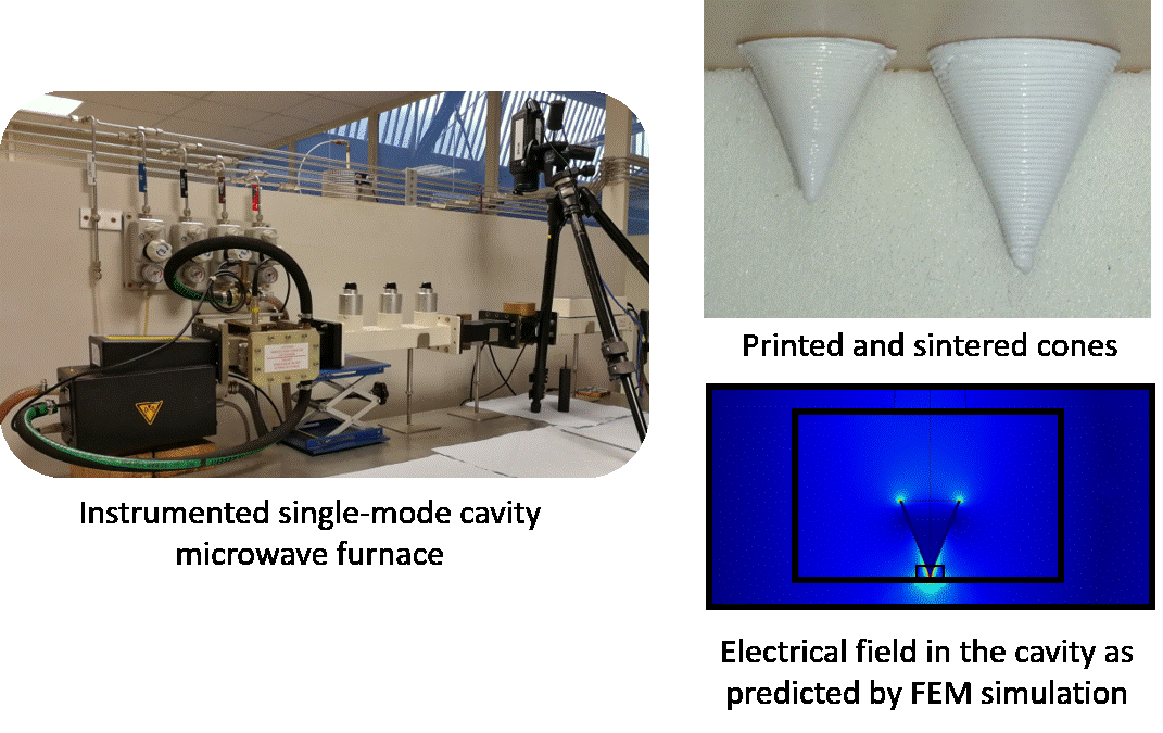
- Field-assisting sintering, i.e. sintering involving an electrical or an electromagnetic field is gaining interest, in particular due to considerable energy and time savings. A particular attention is given to the microstructures generated through those processes and modelling approaches are also developed.
- Injection Moulding of Bulk Metallic Glasses: those materials exhibit interesting properties but one of the main challenge to be overcome is their processabilty. Here an innovative process (patented) is employed to achieve near net-shape miniaturized components.
Electron Beam Melting Additive Manufacturing
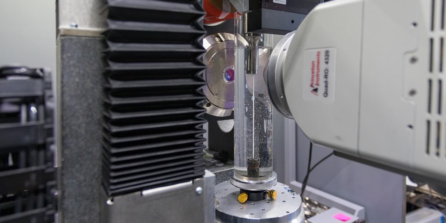
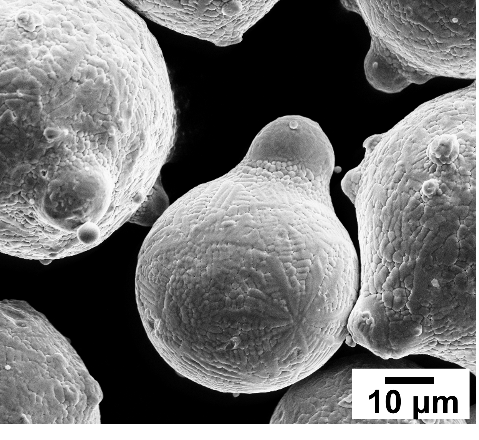
- Powder characterization. We pay attention to the powders (raw materials for powder-bed based technologies) and to their evolution throughout the process: from atomization, to flowability, porosity as well as recyling since morphology and chemical composition might change.
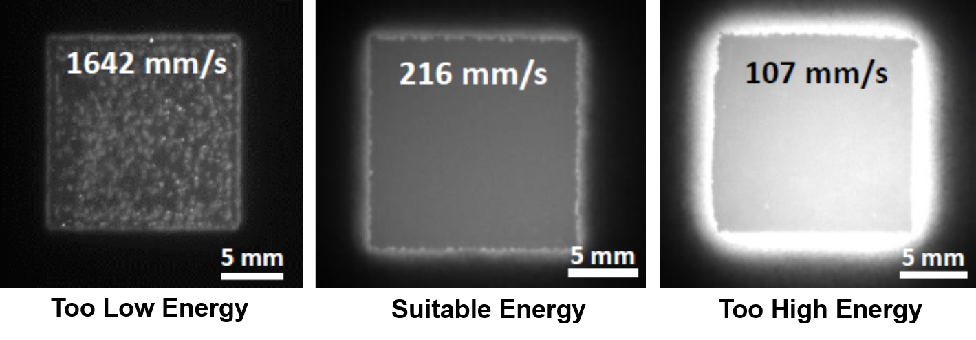
- In-situ process monitoring. We have developed specific set-up allowing to acquire near-IR optical image at every layer of the build in order to detect the presence of typical defects of AM-parts or to detect instable melting conditions, see examples below. Comparison between optical reconstruction based on the images taken at every layer and a full post-mortem non-destructive 3D charcaterization by X-ray microtomography is done to assess the possibilities offered by in situ imaging techniques. This is the first step towards closed loops process monitoring in order to adjust the process at a given layer to heal a defect detected when building the underlying layers.
- Melting strategies. EBM-parts are often built using a standard snake-line melting strategy. We explore new melting strategies as shwon below to alter the microstructures, for instance by modifying the thermal gradient and solidification velocity or by changing the direction of the thermal gradient.

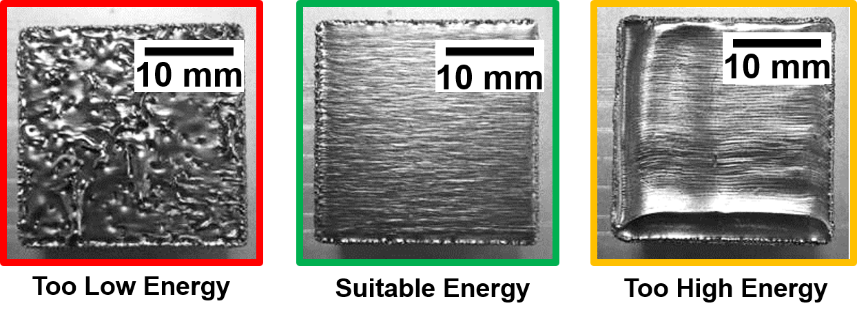
- Materials development. AM-processes and particularly the EBM-technology were applied to very few metals and alloys, mostly Ti6Al4V-alloy, Co-Cr-Mo alloys as well as Inconel 718. Thus there is a need to investigate the possibility to process other alloys and ultimately to design new alloys dedicated to those emerging processing routes. To that end, we have developed an home-made EBM-miniaturized building chamber that fits into existing machines. This allows to take advantage of the same electron gun and atmosphere control (high vacuum) while using a limited amount of powders. This approach clearly speeds up our activities around materials development to quickly identify the suitable processing windows depending on the investigated alloy as illustrated hereafter.
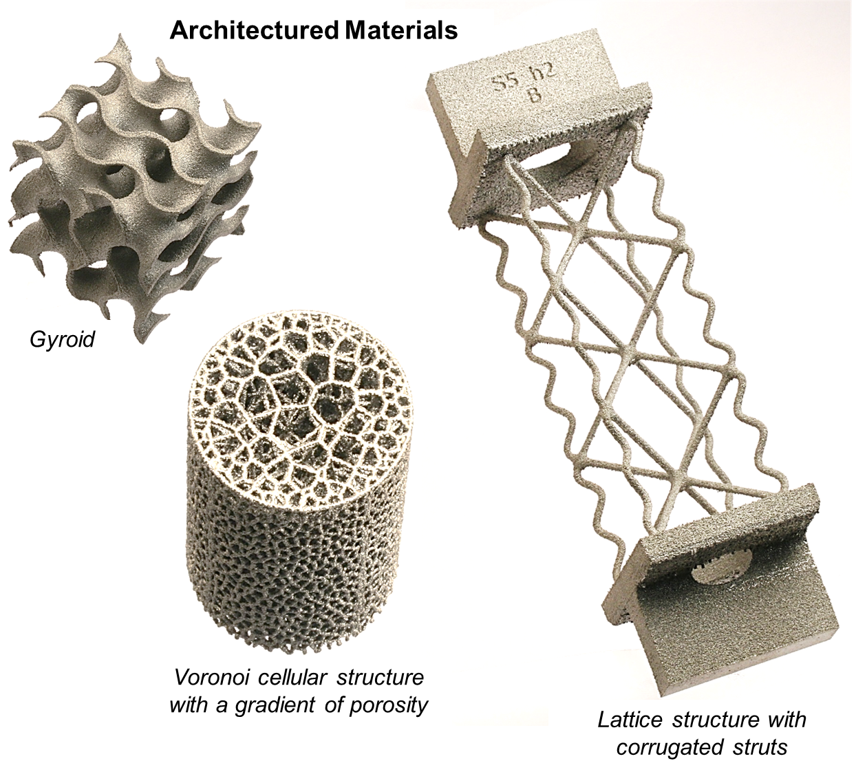
- Architectured Materials. We take advantage of the layer-by-layer process in order to build ophisiticated geometries such as architectured materials including periodic, lattice structures, graded structures as well as more complex architectures using corrugated struts as shown below.
Sinter-based additive manufacturing
Indirect additive manufacturing processes, in which a green part is printed and then sintered, is attracting increasing interest. This activity bridges the gap between the powder metallurgy activity and the additive manufacturing activity in the group. Modeling of the sintering of steel parts shaped by binder jetting was studied in connection with the CETIM. The 3D printing of copper parts by fused deposition modeling (FDM) using MIM feedstocks was also carried out using an in-house printer, in collaboration with the LGP2 laboratory, and shape distortions during sintering were studied. A commercial printing machine will be purchased in early 2020 to further investigate the possibilities of this technique.


Field-assissted Sintering
Sintering processes involving an electrical or electromagnetic field are attracting increasing attention due to energy and time savings they bring and novel microstructures they may produce. We currently work on microwave sintering and flash sintering of ceramic powders.
|
|
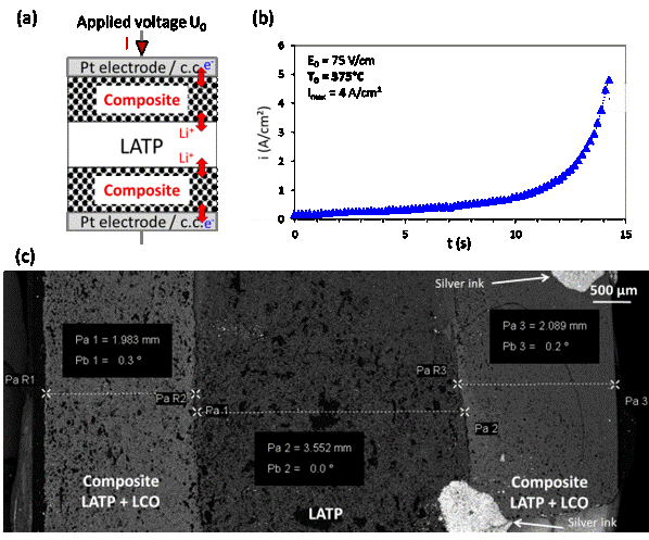 Flash sintering of a three-layer ceramic component possibly used as a solid state battery, BATSOL CEMAM-funded project, coll. LEPMI Grenoble
|
Bulk Metallic Glasses Processing
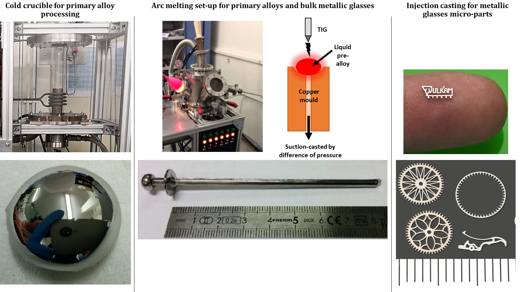
The processing of bulk metallic glasses (amorphous metals) of many different composition relies on theoretical and experimental knowledges of high value at the lab. We can be provided with raw metallic elements of very high purity and prepare the primary alloys (precise compositions) with either a cold crucible device (left) or directly in the home-made arc-melter (middle). Subsequently, bulk metallic glasses of simple shapes (cylindres, plates, cones) can be produced by suction casting in the arc-melter. More recently, a new injection casting process was developed leading to the creation of the VULKAM start-up in order to produce complex net-shaped micro-parts for various industrial applications (right).
Selected Publications
- A. Guyon, D. Bouvard, J.M. Chaix, C.P. Carry. Densification and microstructure changes of micron-size nickel powder during direct induction sintering, Powder Metallurgy 57 (2014) 54-60
- J. Croquesel, D. Bouvard, J.M. Chaix, C. P. Carry, S. Saunier, S. Marinel. Direct sintering of pure alumina in a single mode cavity: Grain size and phase transformation effects. Acta Materialia 116 (2016) 53-62
- E. Bichaud, J.M. Chaix, C. Carry, M. Kleitz, M.C. Steil, Flash sintering incubation in Al2O3/TZP composites, Journal of European Ceramic Society 35 (2015) 2587–2592
- E. Chauvet, C. Tassin, J-J. Blandin, R. Dendievel, G. Martin. Producing Ni-base superalloy single crystal by selective electron beam melting. Scripta Materialia 125 (2018) 15-19
- P. Kontis, E. Chauvet, Z. Peng, J. He, A. Kwiatkowski Da Silva, D. Raabe, C. Tassin, J-J. Blandin, R. Dendievel, S. Abed, B. Gault, G. Martin. Atomic-scale grain boundary engineering to overcome hot cracking in additively manufactured superalloys. Acta Materialia 177 (2019) 209-221
Chercheurs / Enseignants-chercheurs
PhD and post-docs
Edouard CHAUVET (2017)
Guillaume CROSET (2020)
Mathis DUPORT (2022)
Tristan GARNAULT (2020)
Loïcia GAUDILLIERE (2022)
Melek GENC (2021)
Paul HERVIER (2017)
Alexis LENAIN (2017)
Akash SONAWANE (2020)
Alizée THOMAS (2020)
Alexis BURR (post-doc 2019)
Emeric PLANCHER (post-doc 2019)
Collaborations
MATEIS
Université Libre de Bruxelles (ULB)
CRISMAT
LEPMI
Poly-Shape
ONERA
AIRBUS
AUBERT & DUVAL
SCHNEIDER-ELECTRIC


