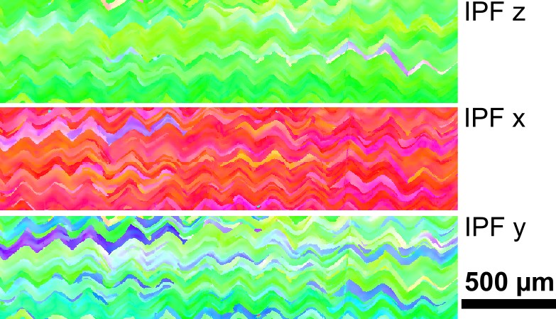
Orientation maps (EBSD) of a copper microstructure obtained by EBM (Electron Beam Melting) additive manufacturing. This wavy microstructure results from a modification of the melting parameters leading to thermal gradient direction changing at each layer (100 µm). The author likes to thank Florence Roubaut for the orientation maps, and Remy Dendievel for an alternative title "To bend copper".
About the author: Alizée THOMAS is a 3rd year Ph.D student in GPM2 group. Her Ph.D, entitled "Development of copper electrical conductors using selective electron beam melting (EBM)", is a CIFRE contract with Schneider Electric.