Electrical properties
Monitoring the electrical behaviour of a material is either a way to better understand its fundamental structure or a mean to enrich its microstructural/mechanical characterisation. These complementary approaches have been widely developed at SIMaP heading toward multi-scale and multi-functional characterisations of most classes of materials (metals, ceramics and semiconductors).
(Fabien Volpi, Marc Verdier)
Electrical-characterization platform
The electrical characterisation platform of SIMaP gathers up-to-date electrical measurement units (for resistive and capacitive measurements) with numerous probing set-ups enabling the testing of various behaviours and geometries (from integrated chips to bulk metals). Most of the probing set-ups are home-optimised: microelectronic-compatible probe station with heating chuck, electrically-functionalised mechanical bending device, Hg-probe system, Van der Pauw/Hall effect set-up, Seebeck set-up,...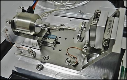
Video of in situ SEM nanoindentation
Selected publications:
(Fabien Volpi, Marc Verdier)
Electrical-characterization platform
The electrical characterisation platform of SIMaP gathers up-to-date electrical measurement units (for resistive and capacitive measurements) with numerous probing set-ups enabling the testing of various behaviours and geometries (from integrated chips to bulk metals). Most of the probing set-ups are home-optimised: microelectronic-compatible probe station with heating chuck, electrically-functionalised mechanical bending device, Hg-probe system, Van der Pauw/Hall effect set-up, Seebeck set-up,...
Aiming at the local electrical characterisation of materials, an AFM apparatus (NanoObserver) dedicated to functional characterisations has been purchased recently (CEMAM funding). Besides the standard modes, several options are available: ResiScope-compatibility, PFM, HD-KFM, Environmental control kit,…
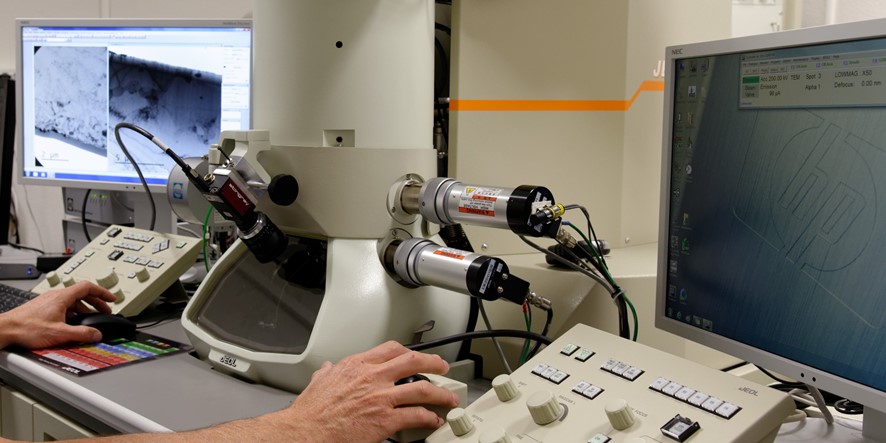
Enhanced nanoindentation: In-situ SEM and electrically-functionalised nanoindenter
In order to support the rising demand for innovative materials optimising functional and structural properties at small scales, an original multifunctional characterization tool has been developed. A commercial nanoindenter has been functionalised for electrical characterisations and integrated into an SEM (on the CMTC platform). This characterisation coupling allows real-time resistive-, capacitive- and piezoelectric measurements during fine mechanical testing. This instrument development has been funded by CEMAM.
Resistive-nanoindentation technique has been successfully applied to the continuous monitoring of the effective indentation contact area which is crucial for the quantitative computation of mechanical properties (hardness and elastic modulus). Capacitive-nanoindentation technique has shown to be an efficient tool for the local measurement of dielectric permittivity of thin films at low frequencies (2MHz). SEM integration allows the testing of small-scale objects, as well as the precise positioning of indentation tests on inhomogeneous materials (see image below).
Video of in situ SEM nanoindentation
Selected publications:
- Fabien Volpi, Lione Cadix, Gregory Berthome, Stephane Coindeau, Thierry Encinas, Nicolas Jourdan, Elisabeth Blanquet Impact of silica-substrate chemistry on tantalum nitride thin films deposited by atomic layer deposition: Microstructure, chemistry and electrical behaviors This Solid Films, vol 669, pp. 392 (2019);
- Fabien Volpi, Huiyuan Lu, Yun Li, Ahmad Ahsan Nawaz, Sylvain Fournier, Fabrice Mege, Muriel Braccini A capacitance-based solution to monitor absolute crack length in four-point bending test: Modelling and experiments Sensors and Actuators A: Physical, vol 254, pp. 145 (2017);
- Solene Comby-Dassonneville, Fabien Volpi, Marc Verdier Electrically-functionalised nanoindenter dedicated to local capacitive measurements: Experimental set-up and data-processing procedure for quantitative analysis Sensors and Actuators A: Physical, vol 294, pp. 185 (2019);
- Solene Comby-Dassonneville, Fabien Volpi, Guillaume Parry, Didier Pellerin, Marc Verdier Resistive-nanoindentation: contact area monitoring by real-time electrical contact resistance measurement MRS Communication, vol 9, pp. 1008 (2019).
Surface chemistry and interface mechanical properties
This axis aims to investigate the effects of surface chemical and structural modification on the mechanical properties of interfaces.
Surface chemistry and structure is modified trough different processes: chemical reaction, physical vapor deposition, or thermal oxidation. The mechanical properties of the interfaces so created is then investigated, particularly in terms of adhesion.
Such studies are based on specific experimental tools in terms of elaboration, such as an in house PVD equipment with in situ stress measurement method, and in terms of characterization, more particularly mechanical characterization dedicated to interface investigation (blister test, 4-point bending test). In parallel to experiments, modelling and numerical simulations coupling the physical, chemical and mechanical aspects are developed in order to improve the understanding of the mechanisms at work and obtain quantitative data.
(Bruno Gilles, Guillaume Parry, Muriel Braccini, Valerie Parry)
Telephone cord buckles-A relation between wavelength and adhesion
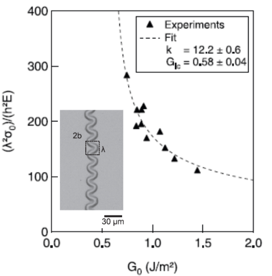
Thin films with low adhesion and large residual stresses may buckle. The resulting morphologies are varied, but one of the most commonly observed is an intriguing oscillating pattern - the so called telephone cord - which has been extensively investigated in the recent years. We have studied the kinematics of formation of telephone cords using a geometrically non-linear plate model and mode dependent interfacial toughness, captured via a cohesive zone. Through extensive Finite Element Simulations, we have demonstrated a simple, non-trivial relation between telephone cord wavelength and interfacial toughness. To validate this prediction, highly stressed Mo thin films were deposited on Si wafers, with a well-defined interface and very reproducible adhesion. Studying the morphology of the resulting buckles for different film thicknesses and stresses, we observed a trend which was fully consistent with our simulation results. From the data fit, an adhesion energy of 0.58+-0.04 J.m2 for the SiO2/Ag interface was inferred, which compares well with literature estimates (see image below).
Frequency-tunable toughening in a polymer-metal-ceramic stack using an interfacial modular nanolayer
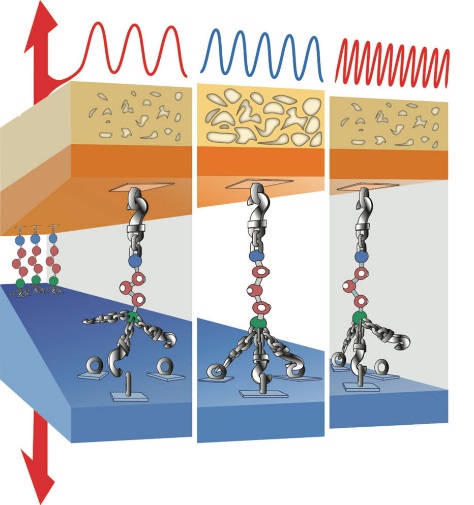
Composites engineered at the nanometer-scale are of interest in a variety of applications including energy, electronics and biomedicine. The performance and reliability of such composites are often governed by the integrity of interfaces between dissimilar materials during loading fluctuations triggered by thermal, electrical and mechanical stimuli. Thus, unearthing and understanding nanoscale phenomena at interfaces during dynamic stimuli, and manipulating them, is a key to designing new materials with novel responses for applications. The work published in Nature Communications shows that the use of a layer of molecules called "nanoglue" can facilitate unexpected mechanical hardening depending on the frequency. These results obtained at the Rensselaer Polytechnic Institute are the result of a collaboration of researchers from different fields of materials science, to which Mr. Braccini, CNRS research fellow at the SIMaP laboratory, participated as part of a stay with Professor Ramanath's team (see image below).
Selected publications:
Surface chemistry and structure is modified trough different processes: chemical reaction, physical vapor deposition, or thermal oxidation. The mechanical properties of the interfaces so created is then investigated, particularly in terms of adhesion.
Such studies are based on specific experimental tools in terms of elaboration, such as an in house PVD equipment with in situ stress measurement method, and in terms of characterization, more particularly mechanical characterization dedicated to interface investigation (blister test, 4-point bending test). In parallel to experiments, modelling and numerical simulations coupling the physical, chemical and mechanical aspects are developed in order to improve the understanding of the mechanisms at work and obtain quantitative data.
(Bruno Gilles, Guillaume Parry, Muriel Braccini, Valerie Parry)
Telephone cord buckles-A relation between wavelength and adhesion
Thin films with low adhesion and large residual stresses may buckle. The resulting morphologies are varied, but one of the most commonly observed is an intriguing oscillating pattern - the so called telephone cord - which has been extensively investigated in the recent years. We have studied the kinematics of formation of telephone cords using a geometrically non-linear plate model and mode dependent interfacial toughness, captured via a cohesive zone. Through extensive Finite Element Simulations, we have demonstrated a simple, non-trivial relation between telephone cord wavelength and interfacial toughness. To validate this prediction, highly stressed Mo thin films were deposited on Si wafers, with a well-defined interface and very reproducible adhesion. Studying the morphology of the resulting buckles for different film thicknesses and stresses, we observed a trend which was fully consistent with our simulation results. From the data fit, an adhesion energy of 0.58+-0.04 J.m2 for the SiO2/Ag interface was inferred, which compares well with literature estimates (see image below).
Frequency-tunable toughening in a polymer-metal-ceramic stack using an interfacial modular nanolayer
Composites engineered at the nanometer-scale are of interest in a variety of applications including energy, electronics and biomedicine. The performance and reliability of such composites are often governed by the integrity of interfaces between dissimilar materials during loading fluctuations triggered by thermal, electrical and mechanical stimuli. Thus, unearthing and understanding nanoscale phenomena at interfaces during dynamic stimuli, and manipulating them, is a key to designing new materials with novel responses for applications. The work published in Nature Communications shows that the use of a layer of molecules called "nanoglue" can facilitate unexpected mechanical hardening depending on the frequency. These results obtained at the Rensselaer Polytechnic Institute are the result of a collaboration of researchers from different fields of materials science, to which Mr. Braccini, CNRS research fellow at the SIMaP laboratory, participated as part of a stay with Professor Ramanath's team (see image below).
Selected publications:
- J.-Y. Faou, G. Parry, S. Grachev, E. Barthel Telephone cord buckles-A relation between wavelength and adhesion Journal of the Mechanics and Physics of Solids, vol 75, pp. 93 (2015);
- M. Kwan, M. Braccini, M. W. Lane, G. Ramanath Frequency-tunable toughening in a polymer-metal-ceramic stack using an interfacial modular nanolayer Nature Communications, vol 9, 5249 (2018).